Surges 9% on Plans for Advanced Chip Packaging Facility")
Key Takeaways
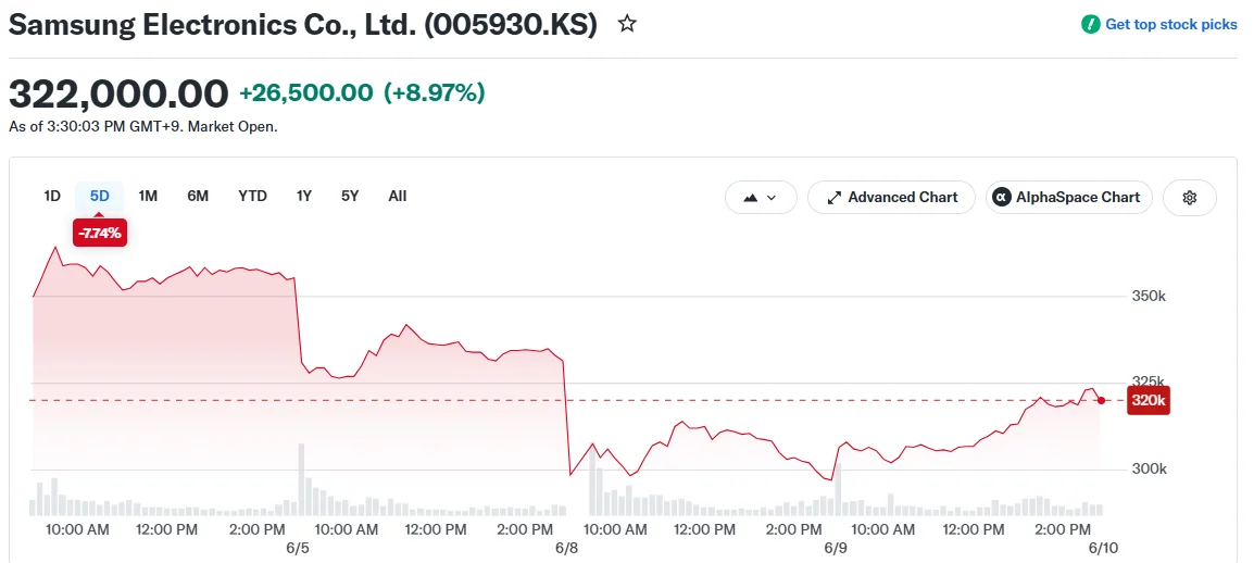
- Shares of Samsung Electronics climbed nearly 9% following reports the tech giant may construct an advanced semiconductor packaging facility in Gwangju, South Korea.
- An official announcement regarding the investment could come during a June 29 gathering between South Korean President Lee Jae Myung and top business executives.
- The proposed plant would strengthen Samsung’s capabilities in advanced chip packaging, a critical segment of the AI semiconductor ecosystem.
- Samsung faces stiff competition from SK Hynix in the high-bandwidth memory sector, which provides essential components to Nvidia, AMD, and Google.
- Samsung recently started delivering sample units of its 12-layer HBM4E memory chip to clients in May.
Shares of Samsung Electronics (005930) surged approximately 9% on Tuesday following a Korea Economic Daily report suggesting the company is evaluating plans to construct an advanced semiconductor packaging plant in Gwangju, located in southwestern South Korea.
According to the publication, which cited anonymous industry insiders, Samsung may unveil this investment strategy during a scheduled June 29 meeting at the presidential residence. The event will bring together South Korean President Lee Jae Myung and executives from the nation’s largest business conglomerates.
Samsung Electronics Chairman Jay Y. Lee is anticipated to participate in the high-level meeting, alongside SK Group Chairman Chey Tae-won. The session’s central theme revolves around implementing a “major shift in growth strategy.”
Samsung has not issued a statement regarding the media report. Officials from the presidential office noted that investment choices remain under corporate jurisdiction.
The Strategic Importance of Advanced Packaging
Advanced semiconductor packaging has emerged as a crucial competitive arena within the chip manufacturing industry. This technology enables producers to vertically integrate and combine multiple semiconductor dies into unified packages, boosting computational power without exclusively depending on transistor miniaturization.

The market for high-bandwidth memory solutions has experienced particularly robust growth. HBM technology vertically stacks multiple DRAM modules and pairs with AI accelerators manufactured by firms like Nvidia. These components play an essential role in powering AI server infrastructure.
Samsung currently provides semiconductor solutions to leading AI technology companies including Nvidia, AMD, and Google — enterprises that are fueling demand for sophisticated memory technologies deployed in artificial intelligence data center environments.
A newly established packaging operation in Gwangju would signal Samsung’s commitment to accelerating capital deployment in anticipation of a semiconductor industry recovery driven by artificial intelligence applications.
The Samsung-SK Hynix Rivalry
Samsung continues its efforts to narrow the competitive distance with SK Hynix, which currently dominates the HBM marketplace. SK Hynix shares also experienced gains on Tuesday, jumping more than 15%.
Last month, Samsung announced it had begun distributing sample quantities of its newest HBM solution, the 12-layer HBM4E configuration, to potential customers. This represents an advancement beyond earlier iterations and demonstrates the company’s determination to maintain competitive positioning.
The upcoming June 29 presidential meeting with corporate leaders could provide the formal platform for Samsung to detail its strategic expansion plans.
Samsung has yet to verify the Gwangju facility project, and the Korea Economic Daily’s reporting draws from confidential industry contacts.
Get 3 Free Stock Ebooks
Discover top-performing stocks in AI, Crypto, and Technology with expert analysis.
- Top 10 AI Stocks - Leading AI companies
- Top 10 Crypto Stocks - Blockchain leaders
- Top 10 Tech Stocks - Tech giants