Commits $13B to Advanced Chip Packaging Facility in South Korea")
Key Highlights
- SK Hynix is committing 19 trillion won (approximately $13 billion) toward a new semiconductor packaging facility in South Korea.
- The facility, designated P&T7, will be situated in the Heungdeok district of Cheongju and focused on cutting-edge chip packaging operations.
- Groundbreaking is scheduled for this month, with operations targeting April 2026.
- The site will manufacture high-bandwidth memory (HBM) chips essential for AI infrastructure and Nvidia’s processing units.
- The company has already launched volume production of advanced memory designed for Nvidia’s forthcoming Vera Rubin AI platform.
SK Hynix disclosed on Wednesday its intention to allocate roughly 19 trillion won — equivalent to about $13 billion — for the construction of a new state-of-the-art packaging fabrication site in South Korea. Designated as P&T7, the facility will be established in Cheongju’s Heungdeok district.
According to a company regulatory submission, construction activities are scheduled to commence this month. This represents one of the chipmaker’s most substantial single-site capital commitments in its history.
The new manufacturing hub will concentrate entirely on sophisticated packaging technologies — the critical assembly process for high-bandwidth memory (HBM) chips. HBM serves as the backbone memory solution for contemporary AI accelerators, including those manufactured by Nvidia’s leading product lines.
As a premier global memory chip manufacturer and crucial Nvidia partner, SK Hynix has experienced dramatic demand increases driven by the rapid expansion of AI data center infrastructure worldwide.
The Strategic Importance of Advanced Packaging
Advanced packaging technology transcends basic manufacturing — it fundamentally controls the velocity and efficiency of data transfer in memory chips. For artificial intelligence applications, this performance factor is paramount.

HBM architecture utilizes vertically stacked memory layers interconnected via microscopic vertical pathways. Executing this intricate process at commercial scale requires both sophisticated technical expertise and substantial capital resources.
The chipmaker indicated it has been accelerating capacity expansion initiatives to satisfy increasing order volumes. Earlier in the year, the company fast-tracked the launch of another memory chip production facility in South Korea for identical strategic reasons.
SK Hynix clarified in its regulatory filing that the planned investment amount remains flexible and may be adjusted based on evolving market dynamics and corporate strategic priorities.
Vera Rubin Memory Module Production Begins
Earlier in the week, SK Hynix announced the commencement of volume manufacturing for a next-generation memory module engineered exclusively for Nvidia’s Vera Rubin AI processor — the successor platform to Nvidia’s Blackwell architecture.
This production announcement arrived merely days ahead of the $13 billion facility revelation, highlighting the aggressive pace at which the company is advancing to secure its supply chain positioning.
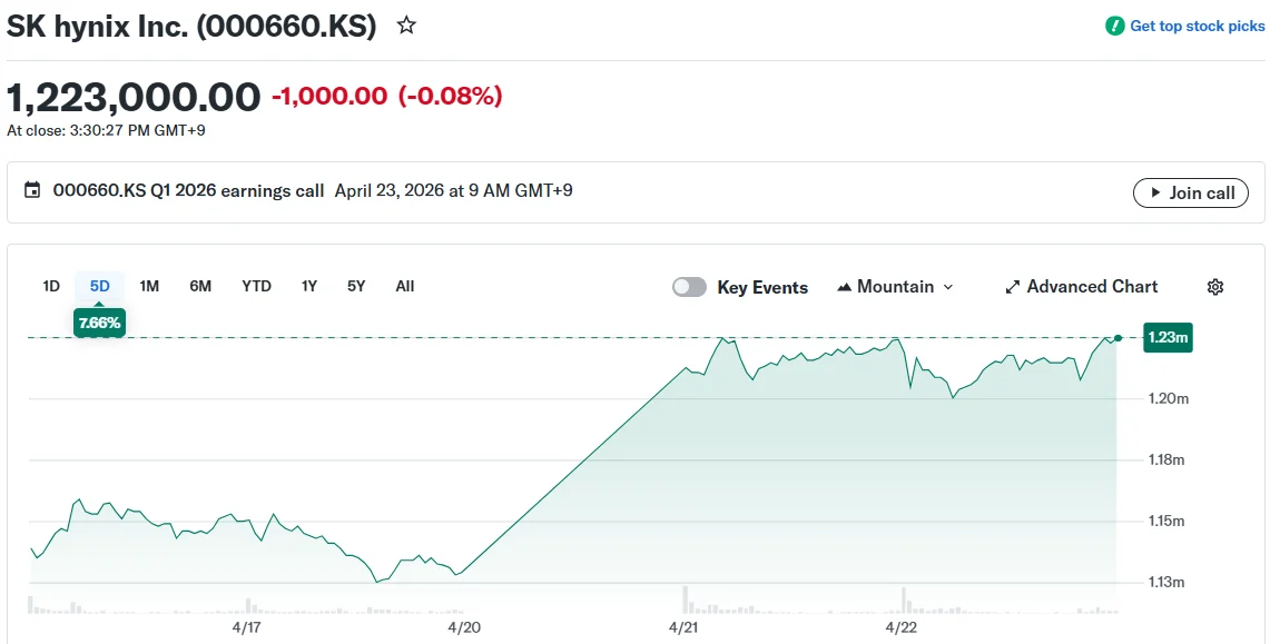
Shares declined approximately 1% on Wednesday in response to the investment disclosure. This modest pullback followed a trading session where the stock had climbed to all-time peak levels.
As of Wednesday’s close, SK Hynix shares trade on the Korea Exchange under ticker symbol 000660. The company has not yet announced a projected completion timeline for the P&T7 manufacturing complex.
Get 3 Free Stock Ebooks
Discover top-performing stocks in AI, Crypto, and Technology with expert analysis.
- Top 10 AI Stocks - Leading AI companies
- Top 10 Crypto Stocks - Blockchain leaders
- Top 10 Tech Stocks - Tech giants