Key Highlights
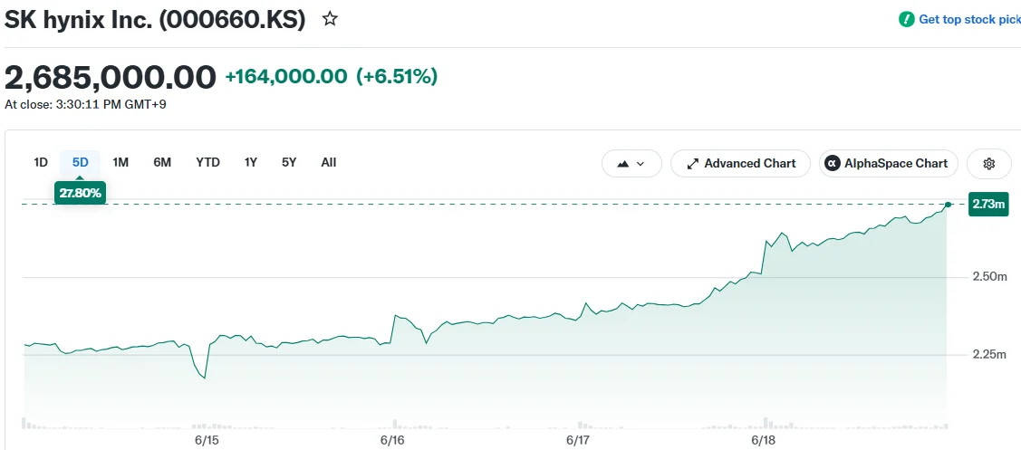
- Shares of SK Hynix climbed 6.51% following confirmation that HBM4E samples reached key partners
- The advanced 12-layer memory module delivers 16Gbps per pin speeds with over 20% enhanced power efficiency versus HBM4
- Using Advanced MR-MUF packaging technology, the chip achieves 48GB capacity with 17% superior thermal management
- SK Hynix maintains its position as Nvidia’s leading HBM provider while Samsung and Micron pursue market share
- Mass production timeline remains undisclosed, with the company emphasizing close collaboration with ecosystem partners
South Korean semiconductor manufacturer SK Hynix revealed on Thursday that it has delivered sample units of its cutting-edge HBM4E memory technology to principal clients, triggering a 6.51% rally in the company’s shares on the Korea Exchange. The positive sentiment extended across the memory sector, with Samsung’s stock advancing 4.62% and Micron gaining 2.20%.
The HBM4E represents a 12-layer high-bandwidth memory architecture specifically engineered for artificial intelligence workloads. The chip achieves peak data transfer rates of 16 gigabits per second per pin while demonstrating power consumption improvements exceeding 20% when compared to the standard HBM4 variant.
High-bandwidth memory modules serve as critical infrastructure within AI accelerators, including those manufactured by Nvidia. These components manage the massive data throughput necessary for training and executing advanced AI systems. Their absence would render large-scale artificial intelligence processing fundamentally impractical.
SK Hynix currently serves as Nvidia’s principal HBM technology provider. While Samsung and Micron continue efforts to narrow the competitive divide, SK Hynix has maintained technological leadership across multiple product generations — spanning HBM3, HBM3E, and progressing through HBM4 to the latest HBM4E.
The semiconductor manufacturer confirmed that the 12-stack HBM4E samples arrived at customer facilities “on schedule,” crediting its accumulated expertise in HBM engineering and manufacturing for enabling on-time delivery.

Technical Advancements in HBM4E
The HBM4E architecture reduces data transfer latency through refined interface specifications and optimized design elements, while ensuring consistent performance under high-bandwidth operating conditions. These characteristics prove essential for AI datacenter infrastructure managing continuous, large-scale computational demands.
SK Hynix employs a production technique designated Advanced MR-MUF — Mass Reflow Molded Underfill — which introduces liquid encapsulation material between vertically stacked chip layers. This methodology enables the company to achieve 48GB capacity within a 12-layer configuration while delivering 17% enhanced thermal resistance compared to HBM4.
Enhanced thermal management capabilities ensure memory modules maintain reliable operation within high-performance computing environments characterized by significant heat generation.
Path Toward Commercial Production
Ahn Hyun, serving as SK Hynix’s President and Chief Development Officer, stated the organization has “laid the foundation to strengthen its AI leadership with HBM4E,” adding that collaboration with industry partners will facilitate market delivery while preserving the company’s standing as a “full-stack AI memory creator.”
The firm refrained from announcing a definitive mass production schedule, indicating only its intention to “work closely with partners for mass production in a timely manner.”
Nvidia’s shares declined 1.33% during Thursday’s trading session, a movement unrelated to the SK Hynix development.
The HBM4E sample distribution builds upon SK Hynix’s proven history supplying HBM3 and HBM3E solutions to the marketplace — product generations that solidified its strategic partnership with Nvidia prior to the introduction of HBM4 technology.
Get 3 Free Stock Ebooks
Discover top-performing stocks in AI, Crypto, and Technology with expert analysis.
- Top 10 AI Stocks - Leading AI companies
- Top 10 Crypto Stocks - Blockchain leaders
- Top 10 Tech Stocks - Tech giants